A simple low cost colour testcard generator
This article first appeared in CQ-TV magazine, issue 201 and modifications were listed in issue 205.
This project was conceived out of two needs. One was to make a very low cost test signal generator, the other was to teach the author how to use programmable logic devices (PLD).
It is doubtful that many involved in the electronics trade have never seen one of these. They come in all shapes and sizes and a multitude of different internal properties. They have become the replacement for 74 series TTL and their CMOS counterparts, allowing their many individual functions to occupy the same slice of silicon. Their logic functions are, however, identical to their predecessors.
In a world where conventional dual-in-line (DIL) chips are becoming scarce, the author was faced with the challenge of learning how to use them or be resigned to using outdated technologies. Having decided to bite the bullet, the next stage was to see what tools were available on the market to teach about and use PLDs. There are several development kits on the market, some being way outside the authors budget but one stood out from the crowd and was easily available at relatively low cost. This is the ISP development kit, sold by Farnell and others. It is designed by and specifically for use with PLDs made by Lattice Semiconductor Corporation. Two sample devices, a simple demonstration board and development software are provided in the kit. The demo board can be used to program the PLDs via a cable that plugs into a PC printer port. Im not going to upset Lattice by divulging the schematic for their board and cable. Suffice it to say that there would be little left over if the demo part of the board were removed. The actual programming hardware is extremely simple.
The development software is quite complex but it comes with extensive documentation. It can do many things that I still havent worked out but the core operations needed to input a design and prepare it for placing on silicon are fairly straightforward. The design can be entered as logic equations or as a schematic using a drawing program. I chose the latter method.
When the design has been entered, it can be simulated to check it works properly. This process is quite easy and allows the design to be checked before committing it to a real device. All you do is draw the input waveforms you expect to feed in to the device and ask it to show its outputs. Pressing the run button provides a display of input, output or both signals in an on-screen logic analyser. If something doesnt look quite right, it is a simple task to revisit the design, change it and try again.
When happy that theres a good chance of it working, the tools for optimising the chip can be run. One of the really nice features of Lattice PLDs is that the software optimises the way the logic functions are placed on the silicon so that the inputs and output pins can be exactly where you want them. In the testcard design for example, the PCB was designed before the logic design was finished. The software was told to connect the pins to match the board layout making the design much easier and allowing a no-links single sided board to be used.
The final step is to put the design into the chip. This is done with another Lattice tool and is very quick. It only takes about five seconds to program and verify the chip. Lattice have designed another really nice feature into their PLDs, they can be erased and reprogrammed over and over again. This was particularly useful while developing the testcard chip as it took many attempts to get it right. Im not going to tell you exactly how many, that would reveal how bad at logic designing I am!
The Testcard Generator.
These are always useful gadgets to have in the shack and not too complicated to consider for a first attempt and PLD design. I had for some time had the idea to try redesigning my existing generator into a single chip. My old generator is based on a design by, I believe, Colin Edwards which was published many years ago. I originally planned to copy the logic structure directly into the new chip but found there was sufficient spare capacity left over to try incorporating a PAL encoder too. This part proved to be more of a challenge.

I confess to delving into old textbooks and browsing the Internet for ages, trying to re-learn things long forgotten about colour encoding. It was a quite enlightening experience and well worth trying yourself if you have a few weeks to spare! What became apparent was that there was no need to use an analogue encoder as all the possible colours from the generator section were at the same level. They are just switched on or off in different combinations to achieve the standard colour bar colours. With this in mind, it is relatively easy to generate the required chroma phases for each primary colour and turn them on only when necessary. For alphanumeric characters, which are always white, the red, green and blue are all turned on together. The relative levels of each colour phase and RGB output (Gamma) is set by a crude but effective array of resistors. These form a simple digital to analogue converter when combined in the transistor buffer stage. The second buffer is simply to remove the effects of loading by whatever you are driving into. Without it the chroma level varies too much as the load impedance changes.
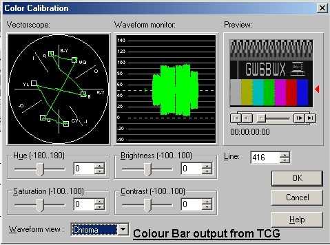
The vectorscope display shows that the final result is actually quite good for such a simple design and comparable with that from far more complicated units.
The first prototype used a crystal oscillator running at twice the colour subcarrier frequency. The circuit has to drive a clean signal at high output level to clock the chip and was found to occasionally flip the ident phase with disastrous results. The design here uses a crystal at four times subcarrier frequency and internally divides it by four. This was found to give far superior results but still demands a high output from the oscillator circuitry. I would advise sticking to the component values given or you may encounter strange encoding effects. The reliability could be improved by adding a buffer stage after the oscillator but this would increase both cost and complexity.
The burst signal timing is not correct but is close enough that none of the monitors or video capture cards I tried noticed anything was wrong. I tried in vain to improve the timing but ran out of silicon on every occasion.
When in operation the board consumes about 120mA from a five volt supply. The PLD is easily damaged if this is exceeded. Because of the problems mentioned earlier about the subcarrier clock levels, the circuit will start to malfunction if the supply drops much below five volts. The prototypes dropped to black and white at 4.5 volts but miraculously still gave a reasonable black and white picture down to about 3 volts. The PLD used is an M4A5-64/32, the 5 indicating its supply voltage rating. There is also an M4A3-64/32 that runs on 3 volts. I have not tried this device but it may allow lower voltage and current operation. The 5V version takes less than one quarter of the power taken by the original discrete component design.
The EPROM contains exactly the same data as used on the discrete design. This makes it compatible with almost all the homemade testcard generators in use today. The only difference you might see is that connections to the topmost four address lines are brought out to pads. The pull-down resistors ensure these are at a logic zero level unless externally pulled high. If the EPROM used is a 2764 or 27128, always connect the pad nearest the corner of the board to the 5V supply. This is because some makes of these devices insist that pin 1 (VPP) is connected to the same potential as the supply pin. For bigger EPROMS, all four pins can be used and up to 16 different testcard patterns selected.
Some of the PLD pins are intentionally left unconnected. These are used only for programming and testing the chip.
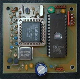
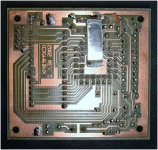

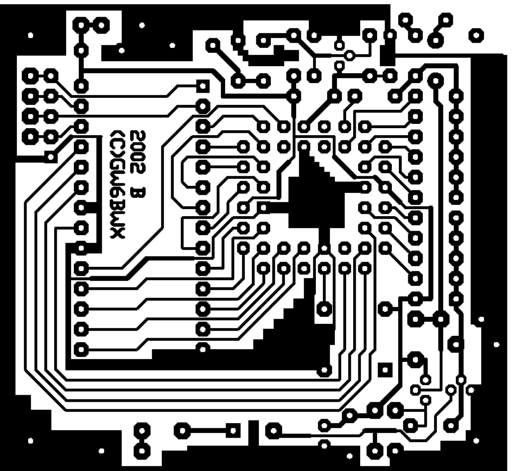
The PCB design I used (which you might recognise from CQ-TV 200) measures 6cm by 6.5cm (about 2.25 x 2.5 inches) so it is quite small. For the purist, the capacitor in series with the crystal can be replaced with a small trimmer to set the subcarrier frequency accurately. The board is laid out to take a fixed capacitor, trimmer or both. If you use your own layout, keep the connections to the clock inputs on pins 11 and 33 of the PLD as short as possible to minimise noise pick-up and RFI radiation. Please note that the photograph of the board shows the revision C layout, since taking it I have made some minor placement changes to make it easier to build. The track layout and placement diagram are for the latest release. The differences between the old and new board are very small. I strongly advise that you add a bridge of tin plate, about 5mm wide between the land in the centre of the PLD and the land near the collector of TR1. Solder the bridge to the two lands, being careful that it doesnt touch any solder pads beneath it. This will reduce noise pick-up on the subcarrier oscillator input to the PLD which improves the colour signal to noise ratio.
| Pin # |
IC1 Name |
IC3 Name |
Pin # |
IC1 Name |
IC3 Name |
Pin # |
IC1 Name |
IC3 Name |
Pin # |
IC1 Name |
IC3 Name |
| |
|
|
|
|
|
|
|
|
|
|
|
| 1 |
A15/ VPP |
GND |
12 |
D1 |
|
23 |
A11 |
GND |
34 |
|
GND |
| 2 |
A12 |
A2 |
13 |
D2 |
|
24 |
A12 |
RED |
35 |
|
|
| 3 |
A7 |
A1 |
14 |
VSS |
BURST_B |
25 |
A8 |
GREEN |
36 |
|
|
| 4 |
A6 |
A5 |
15 |
D3 |
CHR_A |
26 |
A13 |
BLUE |
37 |
|
D2 |
| 5 |
A5 |
A4 |
16 |
D4 |
CHR_B |
27 |
A14 |
A8 |
38 |
|
D4 |
| 6 |
A4 |
A6 |
17 |
D5 |
CHR_C |
28 |
VDD |
CSYNC |
39 |
|
D1 |
| 7 |
A3 |
A7 |
18 |
D6 |
CHR_E |
29 |
|
A9 |
40 |
|
D0 |
| 8 |
A2 |
A3 |
19 |
D7 |
CHR_D |
30 |
|
A11 |
41 |
|
D5 |
| 9 |
A1 |
D7 |
20 |
-OE |
BURST_A |
31 |
|
A10 |
42 |
|
A0 |
| 10 |
A0 |
|
21 |
A10 |
CHR_F |
32 |
|
CLK16 |
43 |
|
D6 |
| 11 |
D0 |
CLK17 |
22 |
-CE |
VCC |
33 |
|
GND |
44 |
|
VCC |
Designing and developing this project has been educational and fun. The outcome is a low cost and very practical device, well worth the pains of climbing the learning curve that it subjected me to. Im still not an expert at logic design but with the tools I now have, I can play and experiment until I get things right. I hope I inspire you to have a go too.
Click HERE for downloadable PCB and PLD programming files.
There are three variants of this project.
The original design is shown on the page below, it closely mimics the performance of the original 'Cropredy' style test card generator and is fully compatible with EPROMs programmed for the old design.
The Mk II version has extra features and slightly better performance but is not fully backward compatible with existing EPROM files. If you are starting from scratch, this is probably the better option, if you are upgrading old equipment you should consider the design below to retain compatibility.
The Mk III version has the same performance as the Mk II but adds the ability to
select one of 16 testcards from a keypad. It also remembers the last selection when powered up again. The buttons above will take you to the later designs.