Making Printed Circuit Boards.
This article first appeared in CQ-TV magazine, issue 200.
In this article, I hope to demonstrate that home made boards are actually quite easy and cheap to make.
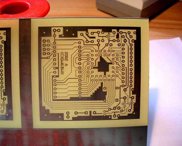
What Im going to describe is the method and equipment I use myself. The photographs and screen snapshot show the prototype of a simple test card generator from design through to testing stages. The principles you see here can be applied to almost any design, whether one of your own or one copied from a magazine or book article. I want to stress that my way of doing things isnt necessarily the most efficient or cost effective way, it just happens to be convenient for me to work in this fashion. The equipment I use to etch the copper is made entirely from salvaged parts and could be improved considerably. Im deliberately not providing any design plans for my home made bits, I leave that to your own ingenuity but by explaining how I do things you should be able to make something at least as good and probably better!
Ill guide you through the stages in sequence:
1. The planning stage.
If you are working from an existing design, such as one published in a book or magazine, skip the next stages entirely and go straight to stage three.
Firstly, make absolutely certain that a PCB is what you need. Often, especially for simple designs, it is easier to use Veroboard or a similar product. Also consider how many copies of your board are likely to be needed. The method I will describe allows you to make an unlimited number of identical copies and if stored safely, the master artwork will be as good as new even after decades of storage. If all you want is a one-off board, bear in mind that the time it takes to design and make it could far exceed the time to assemble it by other methods.
If you have convinced yourself that a PCB is the best solution, start gathering information on the components your design uses. A PCB is, for most designs, nothing more than a neat and repeatable gadget for mounting components, so it is a prerequisite to know how big the components are and where their legs lie with respect to their body outlines. I find it useful to lay the parts out on the bench top and move them around to find the best way of orientating them. The rules here are simple, components must not touch each other or cross over each other on the components side of the board and the same applies for the tracks on the copper side of the board. It is permissible to cross tracks on opposite sides of the board if you use double-sided board but there are complications in doing this. Double sided boards are made as two single sided ones back to back and it takes great care to get the two sides to align properly. Its also very difficult to put copper inside the drill holes so you end up having to solder both sides of the board to connect a track from one side to the other. Take my advice, until you have mastered single sided boards; leave double sided ones well alone!
2. The track layout.
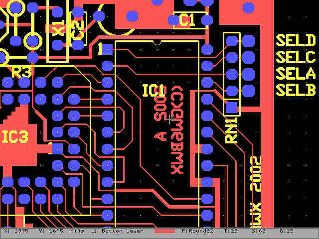
This is the step where a little artistic imagination comes into play. Other than being sensible about the placement of components that have to line up with something else or could interfere with another parts operation, you are free to do just about anything you wish. All you have to do is join the appropriate component legs together with lines. It sounds a lot simpler than it really is but with practice it isnt too difficult. With all but the simplest designs I use a computer with a PCB design program. The one I use is Autotrax from a company called Protel . Its DOS based and by any stretch of the imagination, ancient and rather crude. It does the job though and as a freebie on Protels web site several years ago I cant complain. There are many similar and more up to date packages around these days and their prices are very reasonable. Ive seen someone design a PCB using the Windows Paint program but I would seriously recommend using one designed for the job. What all the design packages give you is a library of component "footprints", the outline of the component when its mounted on the board. They allow you to manoeuvre the outlines until you manage to fit everything into place and then add the lines between the component ends. The real advantage of using a computer is that the components and track lines can be erased or moved after being placed, its akin to moving text around in a word processor but you move parts of a diagram around instead. Some packages will even "auto route" the board for you. All you do is provide a list of components and a list of which pins on them connect together, known as a node list, and the computer takes over and puts the track lines in place. I must confess to having little faith in auto routers, Ive seen some of them pick two points diagonally across the board, join them together and then refuse to connect anything one side of the line to the other because the new lines would cross the diagonal one. I always route boards by hand, I find it gives better results although it can take quite a long time to finish. Manually routing also gives you control over which connections can sensibly lie next to each other, for example, you would have the sense not to run a live mains track parallel to a microphone input signal but an auto router wouldnt realise this was a bad thing to do.
These are the basic dos and donts when laying out the board:
Start by drawing an outline of the board, this gives you a visible boundary to stay within.
Remember to leave holes for mounting the board and leave a gap around the holes for screw heads and mounting pillars.
If any parts must occupy a fixed position, for example a switch that has a shaft that must pass through a hole in a panel, place those parts first. They cant be moved so shuffle the other parts around them.
Leave a space around any parts that get hot so air can circulate and cool them. If heat sinks are being used, remember that no parts can cross the space they occupy.
Leave sufficient gaps around parts and tracks that carry high voltage so the chance of arcing is minimised.
Ensure track lines are "beefy" enough to carry the current expected through them. I use no less than 1mm wide per Amp as a rule of thumb but it also depends on the thickness of the copper on the final board.
Try to fill large gaps between tracks with copper area and if possible connect it to a ground. This helps by providing extra screening, extra heat conducting area and as a bonus it means you dissolve less copper in the production stage so your etching chemicals last longer.
Finally, remember that PCBs are designed from the component side. Imagine you are looking at the components and the PCB substrate is transparent so you can see the tracks on the far side. It is normal, but worrying until you see the reason for it that your design will be a mirror image when you reach the next stage.
3. Transferring the track to copper.
From now on we start to see something resembling the finished product. First, if you bought a huge expanse of board at a rally, cut it down to a manageable size. It ideally should be a little larger than your finished board will be. I always place a thin copper track around the outside edge of my designs so I can use it as a guideline for cutting and filing the board to its actual size.
If you use plain copper board, it should be spotlessly clean. Buy one of those abrasive blocks and gently polish the copper with it until it shines. Then use a solvent to make sure no fingerprints are left on it. I use Ultrasolve ULS for this. Then under dim lighting, spray the board with photo resist paint. The full instructions for this are on the paint can.
Remember that from now on, the board is sensitive to bright light so dont switch the lights on to see if the paint has dried!
I use pre-prepared board. Most of the electronics suppliers stock it. This is board already painted and then protected with a peel-off black plastic coating, which also keeps light off the paint. It is much less hassle to use the ready-made stuff and it keeps for several years if you keep it cool and dry. You can cut it with the protective film still on so the off cut can be kept for use in the future.
The process of transferring the design from computer screen to copper is quite clever and very similar to making photographic contact prints. What you need to do is print the track layout, in black, on to transparent film. I use the sheets designed for overhead projectors which most stationery stores can supply. Be careful though, make sure the brand you choose is designed for use in your kind of printer. Usually, one side of the sheet is glossy and one side is matt, its the matt side you print on or the ink will form droplets on the surface. If, like me you use a laser printer, make sure the film is suitable for laser printing or for photocopying. Both these devices use heat to fix the toner to the film and the wrong sort of transparency will feed into your printer but never come out again. Instead you will find a seriously gummed up printer mechanism, you were warned!
If the printing was successful, you should see black areas where you want copper on the board and everywhere else should be see-through. Hold it up to a light and check for any unfilled areas, if there are any, use a black fibre tipped pen to touch them in. Unfortunately, even the latest printers tend to leave voids when they try to fill large areas.
When the ink has dried or the film has cooled down you can get ready to do some photography. The aim is to expose the paint on the board to a source of ultra violet (UV) light but only in the places we want the copper removed from. The paint undergoes a chemical change when the light falls on it and it becomes soluble in developing solution. Where the black pattern on the film provided shade, preventing the light reaching the paint, it remains insoluble in developing solution.
You need a source of UV light for the next stage. I use a commercially made light box but it is very easy to make your own. You need a box, even my commercially made one is only made from plywood.
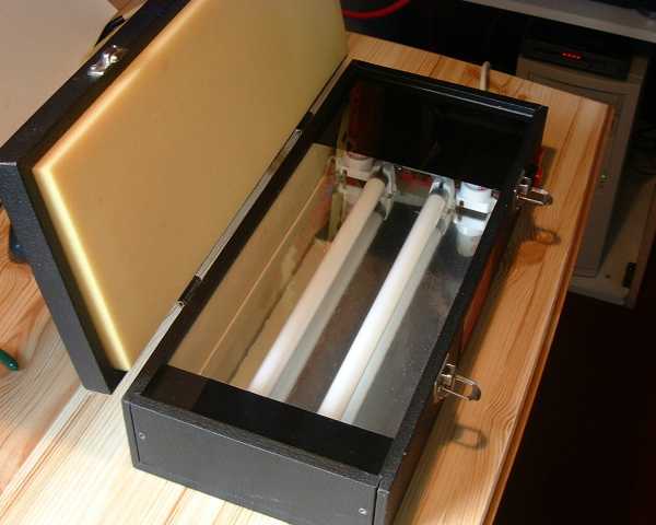
The box needs to be big enough that your biggest PCB can sit in its bottom. Mine is about 15cm front to back, about 30cm side to side and about 10cm deep. This comfortably holds a standard Eurocard (100 x 160mm) board, a size readily available. The top of the box must be clear glass and if possible it should either have a hinged lid or you should have a removable lid that sits flat on the glass. Fit some thin spongy foam to the underside of the lid. The plan is to place the printed film on top of the glass and then place the light sensitised board on top of it. The weight of the lid and the sealing effect of the sponge should hold the board and film flat against the glass. Its quite important if you hinge the lid that it doesnt shift the board relative to the film when you close it or the image will be in the wrong place or even off the edge of the board after exposure. In the bottom of the box you need at least one UV strip tube as a light source these are inexpensive and will last for hundreds of boards. The tubes are available from Farnell, Maplin and CPC amongst others but dont get the ones for disco lighting or EPROM erasers, they are unsuitable for this application. I use two 8W tubes, spaced about 5cm apart as this gives a more even coverage of light. The tubes should be at least 2cm from the glass and each will need a starter and choke. You can add a mains switch or timer if you want but I find that pulling the mains plug out works just as well.
The film goes on the glass with the printed side upward, the board goes on top of it with the painted side downward. This is why the image appears backward on the film; it is re-reversed when placed upside down. Doing it this way means the printed surface is in direct contact with the paint so there is no space for the UV light to scatter and blur the image. Dont forget to remove the protective plastic coating if you use pre-prepared board!
With two tubes, my light box takes about four minutes to fully expose the board, your mileage may vary depending on the number of tubes and quality of glass.
4. Developing the negative.
This stage is simple and quick. You need a plastic tank or tray and some developing solution. Like all the other tools and chemicals, this is easy to get hold of. I buy Farnells ready prepared solution, which is already optimally diluted, but Im almost certain it is actually caustic soda dissolved in water. Remembering that the board is still sensitive to bright light at this stage, remove it from the light box and place it copper side up in the developing tank. Add enough developer to just cover the surface of the board and then swish it gently from side to side so the developer is constantly moving over the paint. Be careful with the chemical, it is corrosive and prolonged contact with skin can cause irritation. Be especially careful not to splash it into eyes where it can cause severe damage very quickly. After about a minute or so you should see the pattern of tracks starting to appear in the paint and after about five minutes the tracks should be clearly visible as paint areas against the plain copper background.
It's safe to leave the board in the developer a little longer than needed for complete removal of the exposed areas paint but dont leave it more than about ten minutes or the unexposed areas may also start to be attacked. Remove the board and rinse it under plenty of cold water. The developer can be saved if you wish and re-used at least one more time. If re-using it the time for development may be a little longer than before as the solution will be partly neutralised. If using the same tray for the next stage you must wash it thoroughly, the etching chemical and developer combine to make an unpleasant brown sludge.
5. Etching the board.
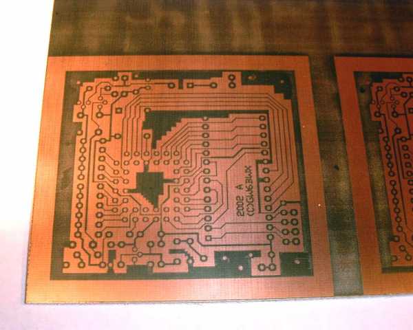
At this stage you should have a copy of your computer artwork painted on a bare copper base. The paint will protect the copper from being dissolved in the etching solution so the copper underneath it will remain and the rest will disappear.
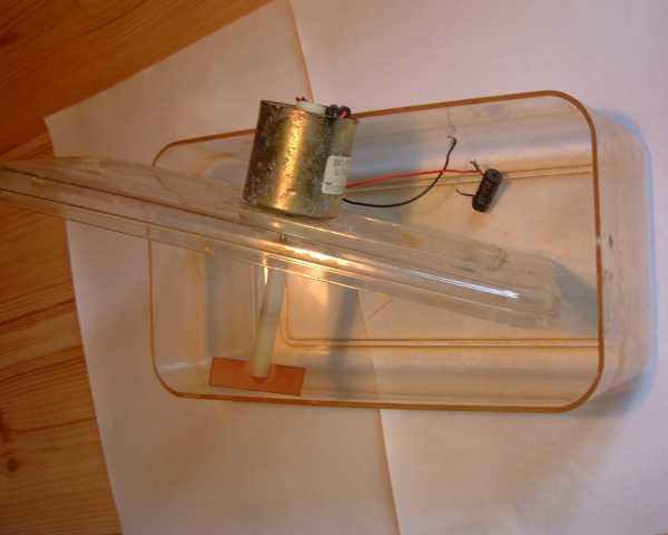
You can do this in normal lighting; the board is no longer sensitive to light after the developing step. Put the board in a tank or tray of etching solution with enough present to cover the board to a depth of about 1cm. I use the same tank as before which was originally a container for chocolates. The solution needs agitating so fresh chemical (Ferric Chloride solution) passes over the copper. I speed the process up by placing the tank in a sink of hot water. The increased temperature speeds up the etching. I also put the lid back on the tank so my "stirrer" can work. This is actually a small 12V motor salvaged from a scrapped video recorder. Its screwed to the top of the lid so its shaft faces downward. The shaft is glued to a plastic rod which has a paddle fixed to its other end. The motor is fed via a resistor to slow it down, it should rotate about four or five times a second. Any faster than this creates the risk of it splashing if the lid is raised.
The intention is simply to keep the solution on the move. In hindsight, I would have fitted two motors and paddles to give better circulation. The etching takes about ten minutes, lift the board occasionally to see if it is finished, this time it isnt wise to keep it in any longer than necessary because the etchant will start to eat under the edges of the paint and reduce the track widths. When finished, thoroughly wash the board in cold water and return the etchant to a plastic bottle so it can be reused. Depending on the amount of copper removed, it should be possible to use it about ten times. Ferric chloride doesnt only dissolve copper; it likes most metals, including stainless steel so take care to keep it from splashing over kitchen sinks.
6. Drilling lots of holes.
You now have a bare substrate with copper tracks in the right places and paint still covering the tracks. Leave the paint there for now; it protects the copper from oxidising.
You can either cut the board to size now or after drilling. I drill first while the board is a little larger and easier to handle. Drilling the holes is laborious and a bit messy. I use a small low voltage drill in a mini-pillar mount. Put a block of wood beneath the board to support it then manoeuvre the board beneath the drill bit.
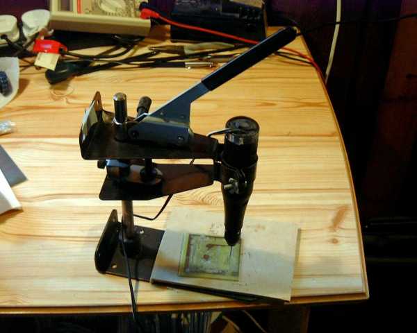
The optimum size of hole for chip legs is 0.6mm and for resistors 0.8mm but larger holes can be tolerated if there is enough copper land surrounding them. It takes quite a long time to drill the holes and a quantity of dust will be created. Its best to use a vacuum cleaner after every 20 or so holes to suck the dust away as it can cause skin irritation. No matter how many times you check all the holes, I guarantee there will be one you missed until you try to fit a component through it!
7. Cleaning up.
Wash the board again after drilling. It is safe to leave the paint in place until you are ready to start assembling the board. The paint is usually "solder through", it acts like flux and burns away when you apply a soldering iron to it. I find it leaves unsightly marks and does little to improve solderability so I use Ultrasolve ULS to dissolve the paint just prior to placing components.
8. This step is entirely optional.
You can if you wish, coat the copper with tin to prolong its life and make it easier to solder to. You need another tank and some tin plating solution for this. Remove the paint and clean the board with ULS then immediately drop it in the plating solution. Leave it for several hours until a silvery film has settled on the copper. Remove the board from the solution and wash it in water. Tin-plating solution is very expensive and although I have plenty, I rarely use it. Making a PCB without plating takes about one hour from computer print to etched board, adding the plating stage makes this much longer and doesnt really offer many benefits. The choice is yours of course. A spray of plastic lacquer or conformal coating does just as well and is quicker than plating.
Using existing designs.
Copying designs from magazines or books is easy if you use the photographic method Ive described. All you do is either photocopy the artwork from the page onto film or use a scanner and printer to do it via computer. You may need to adjust the scale of the copy if the article didnt show it at full size. Scaling is normally a feature of photocopiers and print programs so this shouldnt be a problem. Once you have the design on film, simply go to the UV exposing stage described earlier.
I hope Ive managed to persuade you that no black magic is involved and nothing more complicated than pouring a few chemicals is demanded. It may sound a little complicated at first but in practice the whole operation is quick and gives professional results. The investment in equipment is very modest and it can be used time and time again. What you dont make yourself is easy to find in component catalogues and the chemicals are readily available.
Warning!
The chemicals used to make circuit boards are quite safe to use if handled with respect and stored safely. However, as with most chemicals, misuse can create a hazard and serious injury. The developing solution in particular is caustic and will cause severe damage if it gets into your eyes. Please read the safety instructions on the chemical container labels and be familiar with the actions necessary should an accident occur.
You are advised to wear goggles (eye protection) and waterproof gloves while handling hazardous substances.
I've been making boards for over 30 years without incident but I cannot stress enough that accidents can happen and you should be prepared for them. I do not accept responsibility for other peoples actions!