The mk3 Low-Cost Testcard Generator
Not so much a new Testcard Generator but a variation on the mk1 and mk2 versions elsewhere on this web site.
This version has an added microprocessor which allows the individual EPROM pages to be selected by pressing a single key on a keypad. The selection is stored in non-volatile memory and recalled when the power is turned on. This means that whichever testcard was last selected will be displayed again, even after many years of being powered down. In addition, a voltage regulator circuit has been added to allow the unit to be run from between 10 and 14 Volts as well as the original 5V so it can be powered from a car battery.
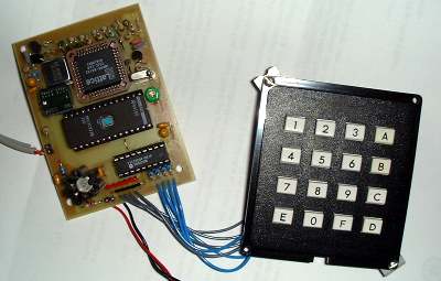
The finished product showing the mk2 board extended to mount the microprocessor and voltage regulator.
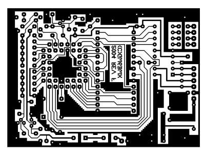
There are some very minor copper track changes to the area previously used in the mk2 version as well as a new area added for the added circuitry. The new dimensions are 80mm x 60mm (approx 3.25 x 2.25 inches).
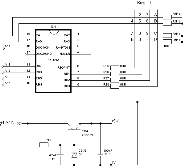
The microprocessor is a PIC 16F84 device. The 16F84A can also be used and so can the 16C84 but the latter should have the polarity of its start-up timer flag reversed for proper operation or it may not initialise properly.
The microprocessor clock input is driven from the EPROM A11 signal. This should be running at 1MHz, regardless of the image being displayed. The code inside the microprocessor scans the keypad, looking for any switch closure. On seeing one, it decodes the keypad signals to decide which key it was then stores its number in its internal EE memory and also sends it to the top address lines of the EPROM.
When power is first applied, the microprocessor reads the last value stored in its EE memory and writes it to the EPROM, re-selecting the last image that was used.
Note that either the mk1 or mk2 versions of the Lattice PLD can be used in this board but take note of the differences outlined on the mk2 TCG web pages.
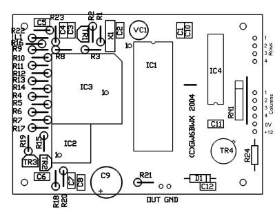
Component placements.
Note: the 4 resistors in line with the row outputs (not shown) are 68R. TR4 is fitted with a small heat sink.
Copper side:
As in the mk1 and mk2, a tin-plate screen must be fitted between the land in the middle of the PLD and the track at the edge of the PCB near TR1 and R2.
Schematic:
The A references are the address lines to the EPROM in the mk1 and mk2 designs.
How it works:
The video generating circuits are identical to the mk1 and mk2versions and are described elsewhere in this site. The new circuits are the voltage regulator and the PIC keypad interface. The regulator is nothing more than a voltage follower, its output being about 0.6V (the B-E voltage) below the transistors base voltage. Using a 5V6 Zener diode to hold the base voltage therefore gives about 5V output. As the transistor dissipates (Vin - 5)*I Watts and I is about 120ma, it has to lose about 7*0.12W of heat - about 0.84W. It therefore needs a small clip-on heat sink to keep it cool.
The firmware in the PIC (IC4) constantly selects each of the keypad rows in sequence. If a signal appears on one of the column inputs to the PIC, the firmware, knowing which row was being driven and which column saw the signal, works out which key was pressed. The key is converted to the EPROM page number then sent to the memory and the EPROM. Every time the PIC is reset, such as at power-up, the most recent stored key number is recalled again. This makes the last selected image reappear on the screen. The four 68R resistors are to protect the PIC should more than one key be held down simultaneously, without them it would be possible to connect the driven row directly to one of the other row outputs which are tied to ground potential.
Click HERE for the PCB files and firmware for the PIC processor.