Audio and Video Distribution Amplifier With Built In Test Generators.
By Brian Kelly. GW6BWX
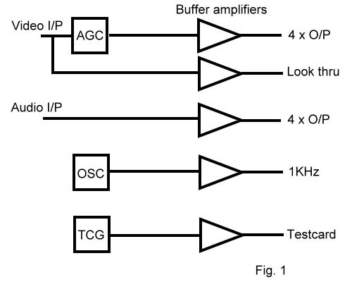
This article describes a device that provides the functions of a one-to-four way distribution amplifier for audio and video signals, a video level stabiliser and produces both a 1KHz test tone and video pattern generator.
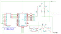
The block diagram of the device is shown in fig 1.
Circuit description
Audio stages:
The distribution stage is one half of IC102 which is configured as a non-inverting amplifier with a voltage gain of 2 (approximately 6dB). The output of the IC is a low impedance point so each of the four outputs sees only the series resistance of R101 to R104 as it's impedance. When terminated with another 1K load, a potential divider is produced in which the voltage is halved, taking it back to the same level as fed to the amplifiers input. Note that within reason, the values of the output resistors can be changed to provide different output impedances. For example changing from 1K to 600 Ohms would drop the impedance to 600 Ohms. The output resistors can be mixed values but to prevent overloading the IC102, I would suggest that no single resistor should be less than 200 Ohms and their combined parallel value should not be lower than 100 Ohms.
The test tone generator is IC101 and the other half of IC102. The 1KHz tone is generated by dividing the frequency from a 4.096MHz crystal oscillator by two, twelve times. All this is done inside IC101. The result is a 1KHz square wave which is then passed through a low-pass filter to remove higher harmonics leaving a close approximation to a sine wave. IC102 is a buffer to reduce the load on the LPF and as it's feedback can be controlled with VR1, the output level can be set as required. I suggest setting the level to 1V peak-to-peak with the output connection terminated with a 1K resistor to ground. As with the distribution stage, it is possible to change the output impedance by adjusting the value of output resistor R105.
Video Stages:
The video input is terminated by R130 to match standard 75 Ohm cable. From here it takes two routes, the buffer stage feeding R117 provides look through and is a replica of the input signal. The other route is through IC103 which is a dedicated video level stabiliser. The chip a Maxim MAX7450 is configurable by two links to enable or disable the AGC function and to set the overall gain to x1 or x2. For normal operation, the AGC should be enabled and the gain set to x2. This gives a stabilised 2V peak to peak video signal at the top of the output level potentiometer. Note that this control is mounted on the front panel, not the PCB. The AGC will keep the level constant with inputs ranging from about 0.5V to 1.5V p-p. The wiper of the control will normally be set about half way to give 1V output but it will adjust between nothing and twice standard video level as required. IC104 and IC105 are driven in parallel and are to give sufficient current gain that four 75 Ohm outputs can be driven simultaneously.
Test Pattern Generator:
This is a modified version of the highly successful TCG Mk2 design which is fully described in CQ-TV magazine and on this web site. The only differences between the original design and the one used here is that the pattern select pins on the EPROM are all tied high (+5) as only one pattern should be needed and the output buffer stage has been replace by half of IC106. The video level can be set by adjusting VR2 and should normally be 1V p-p with the pattern output terminated with a 75 Ohm load.
Testing:
Connect the level potentiometer, set it to full rotation (maximum level) and set VR1 and VR2 to mid position. Set the two links so the gain is x1 and AGC is disabled. Temporarily link the output end of R120 to the video input pin (junction of R130 and C109) with a wire. Connect a 75 Ohm resistor from the output end of R109 to ground and look at the signal across it with an oscilloscope. If an oscilloscope is not available, a television monitor can be used instead of the resistor but ensure nothing in the TV itself provides automatic level adjustment as this will hide the operation of the on-board AGC function. The contrast of the TV picture will give an indication of the video level leaving the unit. Turn on the power source, this should be more than 8V positive and negative but less than 15V.
If all is well, a video signal from the pattern generator will appear, if using a TV monitor a locked but possibly washed out picture should be seen. Set VR2 to give a reasonable quality picture (about 1V p-p on the 'scope), the exact setting isn't important at this stage.
Turn the level control to half way, the video should be about 0.5V p-p and the picture will fade, possibly losing sync as well. Move the link to set the gain to x2. This will double the video gain and restore the picture seen before. On an oscilloscope the level should be restored to 1V again.
Now move the other link so the AGC is enabled. Ignore any change in level as the link is moved. Turning VR2 should now make little difference to the level except at extreme ends of it's rotation. If the level (or contrast) remains essentially constant over most of the control range, the AGC is doing it's job.
Remove the wire link. For the next steps it is far better to use an oscilloscope than a monitor as the reference levels need to be fairly precise. Move the 75 Ohm resistor to the output end of R120 and adjust VR2 until the video level is 1V p-p across it. Next, connect a 1K resistor from the output end of R105 to ground and connect the oscilloscope across it. Adjust VR1 so the waveform is 1V p-p. You will probably have to use a lower oscilloscope timebase speed to see this waveform.
That's it. You now have a testcard generator, test tone generator and distribution amplifiers at your disposal.
Please note that the video produced by the pattern generator is to PAL 625 line / 50 Hz frame standard. Unfortunately, I have no NTSC test equipment here and my TV auto-adapts to just about anything I feed it so confirming NTSC standards are reached would be difficult. As far as I know, replacing the 17.73447MHz crystal with a 14.318MHz one and reprogramming the EPROM should make it work in NTSC countries.
Anyone want a challenge....
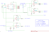
Clicking on the images above will open PDF versions of the schematic diagrams.
Construction:
The PCB is relatively easy to build. Apart from the usual anti-static precautions when handling the integrated circuits everything is robust and easy to work with. The only awkward component is IC103 which is only available in a surface-mount package. The underside of the IC has a bare metal area which should be connected to the same point as pin 4. As far as I can tell, the reason for this is to provide better heat conduction away from the chip and into the PCB. In this application, the load on IC103 is the 1K Ohm level potentiometer rather than the 75 Ohms it would normally work with and the heat generated is therefore a little lower than normal. It is still best to connect the base pad if possible and the best way to do this is to pre-tin the PCB copper with a thin, level layer of solder then with the IC held in position, apply heat to the PCB as close to the chip as possible . Let the solder melt for about three seconds, this should be long enough for the flowing solder to bond with the underside of the IC. The pins can then be soldered as usual. Run a wire link from both crystal cans to ground, this will improve frequency stability, reduce stray radiation and provide a more mechanically secure mounting.


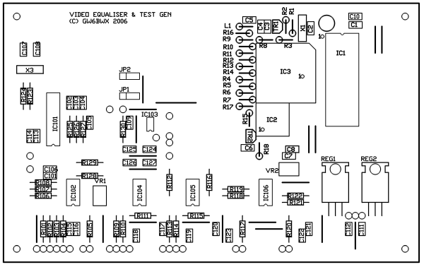
The assembled board, note that IC103 is on the underside (copper side).
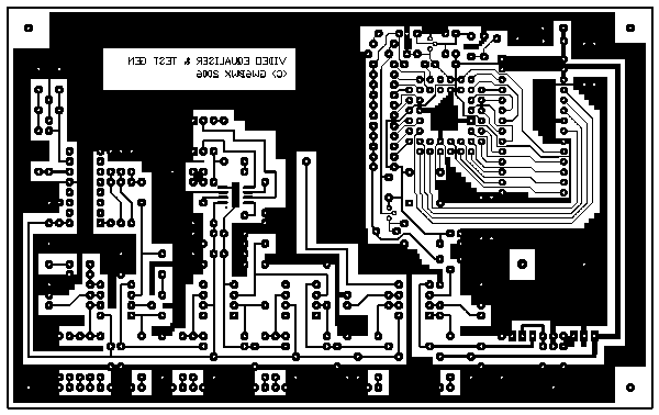
Copper and component layouts.
Click here for high resolution, full size images. File names begin with "video_eq"